- 您现在的位置:买卖IC网 > Sheet目录346 > NCP5050MTTXG (ON Semiconductor)IC LED DRIVR PHOTO FLASH 10-WDFN
�� �
�
�NCP5050�
�The� P� VIN� input� pin� need� to� be� bypassed� by� a� X5R� or� an�
�equivalent� low� ESR� ceramic� capacitor.� Near� the� P� VIN� pin� at�
�least� 4.7� m� F� 6.3� V� or� higher� capacitor� is� needed.�
�Also� a� particular� care� must� be� observed� for� DC� ?� bias�
�effects� in� ceramic� capacitor.� Actually� smaller� the� case� ?� size�
�and� higher� the� DC� bias� voltage,� the� bigger� drop� in�
�capacitance.� For� a� stability� viewpoint� the� percentage� drop� in�
�capacitance� for� the� chosen� input� or� output� operating� voltage�
�must� be� limit� to� 20%.� Some� recommended� capacitors�
�include� but� are� not� limited� to:�
�1.0� m� F� 25� V� 0805�
�TDK:� C2012X5R1E105M�
�4.7� m� F� 6.3� V� 0805�
�TDK:� C1608X5R0J475M�
�Schottky� Diode� Selection�
�An� external� diode� is� required� for� the� boost� rectification.�
�The� reverse� voltage� rating� of� the� selected� diode� must� be�
�equal� to� or� greater� than� the� maximum� output� voltage.� The�
�average� current� rating� of� the� diode� must� be� greater� than� the�
�maximum� output� load� current.� The� peak� current� rating� must�
�be� larger� than� the� maximum� peak� inductor� current.� It� is�
�recommended� to� use� a� Schottky� diode� with� lower� forward�
�voltage� to� minimize� the� power� dissipation� and� therefore� to�
�maximize� the� efficiency� of� the� converter.�
�Also� a� particular� care� must� be� observed� for� parasitic�
�capacitance� versus� reverse� voltage� and� leakage� current�
�versus� junction� diode� temperature.� Both� parameters� are�
�impacting� the� efficiency� in� low� load� condition� and� switching�
�quiescent� current.�
�Some� recommended� Schottky� diodes� include� but� are� not�
�limited� to:�
�ON� SEMICONDUCTOR:� MBR130LSFT1G�
�ON� SEMICONDUCTOR:� MBR120LSFT3G�
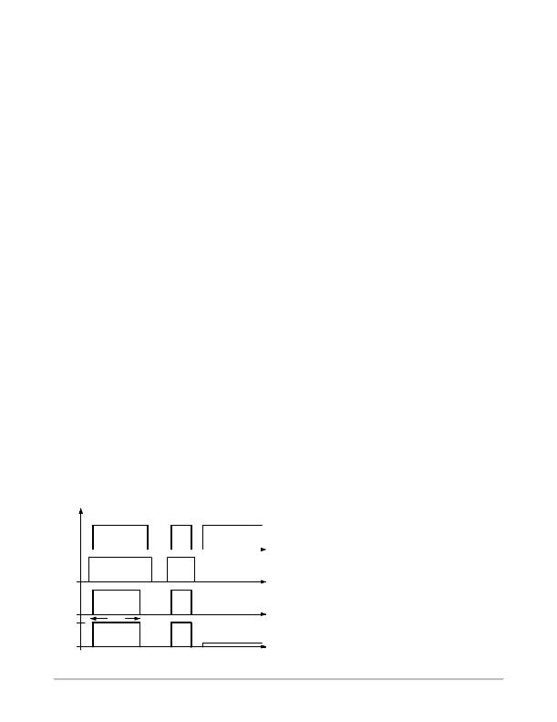
�Timeout� Protection�
�To� avoid� a� failure� in� LEDs� caused� by� a� timing� violation� in�
�Flash� Mode� (CM� high),� a� timeout� function� turn� off� the�
�output� after� 1.2� second.� Any� rising� edge� of� CTRL� reset� this�
�function.� In� torch� mode� (CM� low)� this� circuit� is� disabled.� For�
�the� logic� diagram� please� refer� to� Figure� 25� below.�
�CTRL�
�CM�
�Timeout�
�Overvoltage� Protection� (OVP)�
�The� NCP5050� regulates� the� load� current.� If� there� is� an�
�open� load� condition� such� as� a� loose� connection� to� the� White�
�LED,� the� converter� keeps� supplying� current� to� the� C� out�
�capacitor� causing� the� voltage� to� rise� rapidly.� To� prevent� the�
�device� from� being� damage� and� to� eliminate� external�
�protections� such� as� zener� diode,� the� NCP5050� incorporates�
�an� OVP� circuit,� which� monitors� the� output� voltage� with� a�
�resistive� divider� network� and� a� comparator� and� voltage�
�reference.� If� the� output� reaches� 22.5� V� (nominal),� the� OVP�
�circuit� will� detect� a� fault� and� inhibit� PWM� operation.� This�
�comparator� has� 1.0� V� of� hysteresis� so� allow� the� PWM�
�operation� to� resume� automatically.� when� the� load� is�
�reconnected� and� the� voltage� drops� below� 21.5� V� (nominal).�
�Undervoltage� Lock� Out� (UVLO)�
�To� ensure� proper� operation� under� all� conditions,� the�
�device� has� a� built� ?� in� undervoltage� lock� out� (UVLO)� circuit.�
�During� power� ?� up,� the� device� will� remain� disabled� until� the�
�input� voltage� exceeds� 2.4� V� (nominal).� This� circuit� has�
�100� mV� of� hysteresis� to� provide� noise� immunity� to� transient�
�conditions.�
�Thermal� Considerations�
�Careful� attention� must� be� paid� to� the� internal� power�
�dissipation� of� the� NCP5050.� The� power� dissipation� is� a�
�function� of� efficiency,� input� voltage� and� output� power.�
�Hence,� increasing� the� output� power� requires� better�
�components� selection.� For� example,� should� one� change�
�inductors:� larger� inductor� value� (in� micro� Henri)� and/or�
�lower� DCR� may� improve� efficiency.�
�The� exposed� thermal� pad� that� is� designed� to� be� soldered�
�to� the� ground� plane� to� used� the� PCB� as� a� heat� ?� sink.� This�
�ground� should� then� be� connected� to� an� internal� copper�
�ground� plane� with� thermal� via� placed� directly� under� the�
�package� to� spread� out� the� heat� dissipated� by� the� device.�
�Finally� the� NCP5050� is� switched� off� to� protect� the� device�
�if� junction� temperature� exceeds� 160� °� C.� When� the� junction�
�temperature� drops� below� 140� °� C,� normal� operation� will�
�resume.�
�Flash�
�1.2s�
�Current�
�Torch�
�Figure� 25.� Timeout� Operation�
�http://onsemi.com�
�12�
�发布紧急采购,3分钟左右您将得到回复。
相关PDF资料
NCP5111DR2G
IC DRIVER HI/LOW SIDE HV 8-SOIC
NCP5304DR2G
IC DRIVER HI/LOW SIDE HV 8-SOIC
NCP5355DG
IC DRVR SYNC BUCK MOSF 12A 8SOIC
NCP5359ADR2G
IC MOSFET GATE DVR DUAL 8-SOIC
NCP5359DR2G
IC GATE DRIVER VR11.1/AMD 8-SOIC
NCP5360RMNR2G
IC DRIVER MOSFET 56QFN
NCP5366MNR2G
IC DRIVER MOSFET DFN
NCP5369MNR2G
IC DRIVER MOSFET DFN
相关代理商/技术参数
NCP508
制造商:ONSEMI 制造商全称:ON Semiconductor 功能描述:Very Low Noise, Fast Turn On, 50 mA Low Dropout Voltage Regulator
NCP5080
制造商:ONSEMI 制造商全称:ON Semiconductor 功能描述:Xenon Photoflash Capacitor Charge with Photo Sense Interface
NCP5080 AX95A WAF
制造商:ON Semiconductor 功能描述:
NCP5080MUTXG
功能描述:LED照明驱动器 HI VLTG BOOST DVR 2.7-5.5V RoHS:否 制造商:STMicroelectronics 输入电压:11.5 V to 23 V 工作频率: 最大电源电流:1.7 mA 输出电流: 最大工作温度: 安装风格:SMD/SMT 封装 / 箱体:SO-16N
NCP508MN15TBG
制造商:ONSEMI 制造商全称:ON Semiconductor 功能描述:Very Low Noise, Fast Turn On, 50 mA Low Dropout Voltage Regulator
NCP508MN18TBG
制造商:ONSEMI 制造商全称:ON Semiconductor 功能描述:Very Low Noise, Fast Turn On, 50 mA Low Dropout Voltage Regulator
NCP508MN25TBG
制造商:ONSEMI 制造商全称:ON Semiconductor 功能描述:Very Low Noise, Fast Turn On, 50 mA Low Dropout Voltage Regulator
NCP508MN28TBG
制造商:ONSEMI 制造商全称:ON Semiconductor 功能描述:Very Low Noise, Fast Turn On, 50 mA Low Dropout Voltage Regulator